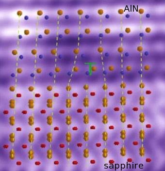
Interface Science Example
- Atomic resolution Z-contrast image of an interface between AlN and sapphire (Al2O3) with overlayed atomic structure model. This materials system is the underlayer for GaN the material of modern light emitting diodes (LED). The lattice parameters of the two materials (AlN and saphire) are different and dislocations accomodate this difference. Dislocations alter the electronic and mechanical properties of materials.
- The understanding of the relationship between materials and the atomistic structure of interfaces is the goal of interface science, a subset of materials science.
- We use modern transmission electron microscopy and ab initio density functional materials simulations to understand the reasons why a specific atomic structure occures at an interfaces. We then to try to alter this structure and with it the materials properties.
